
Cheap Smart Speaker Teardown part 1
Prelude: its been a while. Not that I’ve done nothing, but I kind of dropped the habit of writing publicly about stuff here. Some stuff I wrote up in standalone GitHub repos as well.
Introduction
Last month I picked up a cheap smart speaker from a local electronics retailer and this weekend I was rained in, so took the opportunity to have some fun and practice doing a teardown and firmware dump.
The eventual objective is to see if I can repurpose it to do what a Raspberry Pi might do; these devices typically have Wi-Fi, Bluetooth, audio input and output, some LEDs and a battery, which makes them useful adjuncts to my homebrew home automation setup.
Scope
I have been trying not to buy so much junk the last while, but in this case the thing was on sale for $29 and the long range weather forecast hinted at yet more rain and storms, so I figured the next weekend if I was not able to get out or into the garden I’d do another teardown, and this time, also, write it up… this weekend, it definitely rained. A lot. And the wind… so I had a good chunk of time. I’m ever cognisant of the rabbit hole though, so the scope here is limited to the physical tear down, black box reconnaissance, and dumping the firmware and a preliminary attack surface analysis. I would expected there to be opportunity to do some network analysis oft the running system and also to reverse binaries, but that may be a project for the future. Or not, as there are plenty of activities to attract attention… and hopefully the weather will finally clear as we head into summer.
Objective
Given the scope and timeframe, I want to gain access to a terminal (if possible) and dump the firmware, ideally without resorting to a soldering iron (if possible - at present my lab is in a state where I’m not currently equipped to desolder more than an 8-pin SOIC flash), and take a stab at where to head next.
Secondary objective if at all possible, is disassemble it in a way I can put it back together later :-)
Preparation & Operating Theory
I’m working in the following order: tear down, power up, gain access, dump firmware.
I have my trusty Raspberry Pi 400 which I serve as a serial terminal, and perhaps a Wi-Fi Access Point.
In case it does an automatic firmware update before I’m ready, I don’t want it connecting to the Internet, or linking an account; notably, it appears to just require the google home and assistant app. So later, there will be precautions for that.
According to the product instructions, I should be able to turn it on then find it with google home. I wont be doing that, so I’m going to try Bluetooth scanning and Wi-Fi scanning - often IoT devices will expose an open Wi-Fi AP for the initial pairing. I will make sure it doesn’t connect to my normal AP, I don’t want it accidentally upgrading the firmware.
The target device was manufactured in 2017, which explains why it was on clearance; and perhaps there is a good chance of some legacy security vulnerabilities which may prove useful in the future.
Part 1 - Physical Teardown & Photo Essay
This looks like a not-completely-rubbish product on the outside, it would not look out of place in a high brand department store rather than the cheap stuff you find at Aldi or Kmart. It supports Home Assistant for issuing commands, and Chrome Cast, and can also operate as a plain old Bluetooth speaker. Made in China of course.
This device feels like reasonable quality when you pick it up. It has a strap that feels not-fragile, and the specification claims to be IPX6 for splash resistance. It has a nice weight and looks like it might not completely break the first time you drop it on a concrete floor. There are four buttons for operation, and coloured LEDs. And one assumes, a speaker and microphone(s).
(insert picture)
The manufacturer has also learned a thing from Apple in how neatly it was packaged.
(insert picture)
On turning it over, there is one obvious screw cover, so I gently unstuck it. The tool shown is from a mobile phone repair kit.
(insert picture)
However, that screw only seems to connect the strap, and also it is free-wheeling after I loosen it. Given the moisture-resistant nature of the device, I don’t think that one actually opens it anyway. I confirmed my suspicions this was a red herring, when I started playing at the edge of the circular padding on the base of the device, which turned out to also be a fat sticker. I peeled that off and exposed four more screws. Also a hole with a clear sticker, which I’ll get back to later.
(insert picture)
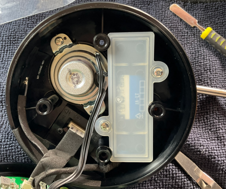
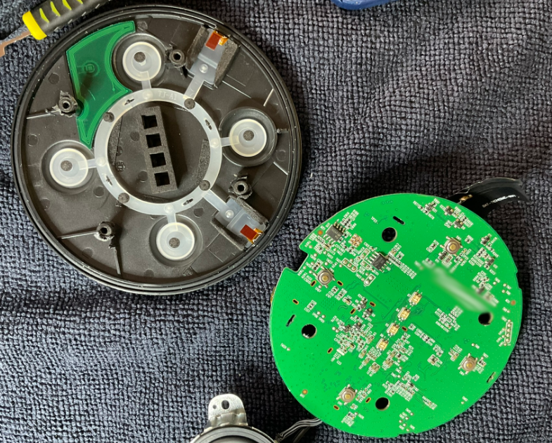
With the screws removed, we can see inside. The enclosure has two parts, with a PCB in the lid, with the buttons and LEDs, with cabling connected to components in the base.
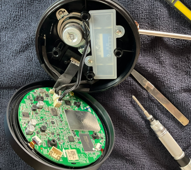
There is a speaker, which actually looks (and later, felt) quite good quality. There is also a compartment for the battery, part of the IPX6 construction.
I was then able to separate the enclosure halves. A wireless antenna (I’m assuming, Wi-Fi) was attached with a sticky flex PCB antenna to the base, with a hot glue glob holding the U.FL connector to the PCB. The speaker was screwed to the top. The battery is an 18650, 3.7volt 2600mAh. The inner container it was in has a rubber seal, presumably for IPX6 protection. There is a flex cable to small PCB somehow entrapped in the base, which has a micro-USB connector for recharging.
The main PCB has a metal can over something, either the main processor chip, and/or the Wi-Fi+Bluetooth circuitry.
(insert picture)
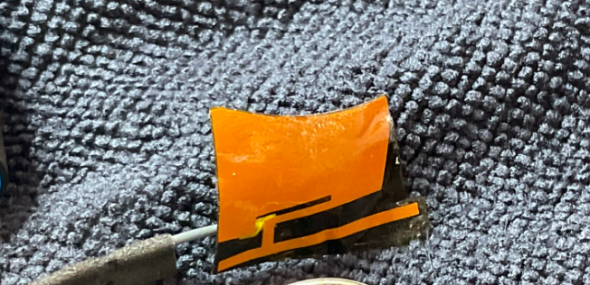
This is a closeup of the antenna.
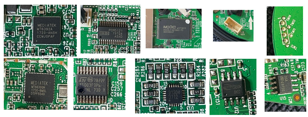
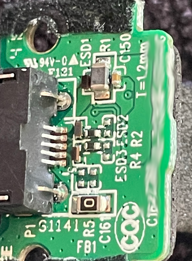
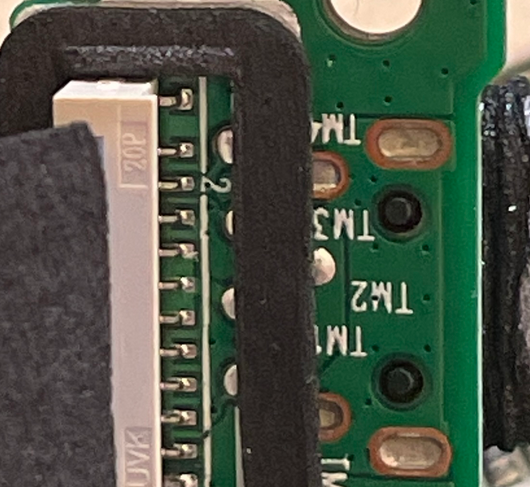
At this point I took photos of all the IC’s on the PCB so I can try and identify them later. The photo also shows 2 from the back - I’ll discuss how I got to that shortly - and an unused connector (and the back of it)
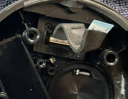
To get to the back, I had to be a bit careful - there were no screws, but I could see plastic lugs, and also the structure the enclosure screws connected also comes through the PCB. There are also two flex-connectors connecting the PCB to the base. I realised that there was some kind of rubber stuff or maybe tape, making the structures a very snug fit. I carefully cut this away, and then after disconnecting the two flex connectors, very carefully and slowly rocked the PCB until it finally came up over. The last thing I wanted to do was crack something!
The lid has lighting duct, for LED display, and two microphones, to which the flex cables connect. There are four buttons on the PCB bottom, and a plethora of test points, which bodes well.
Now I started looking for possible methods to access the system. There is that unused connector, it is only labelled with test points but it could be some kind of JTAG or SWD port, or something totally unrelated, or maybe even a USB port. But the holy grail is a serial port. Thankfully it turned out that I had an easier job, as there was a UART label. Only problem: no PCB points or connectors near the label!
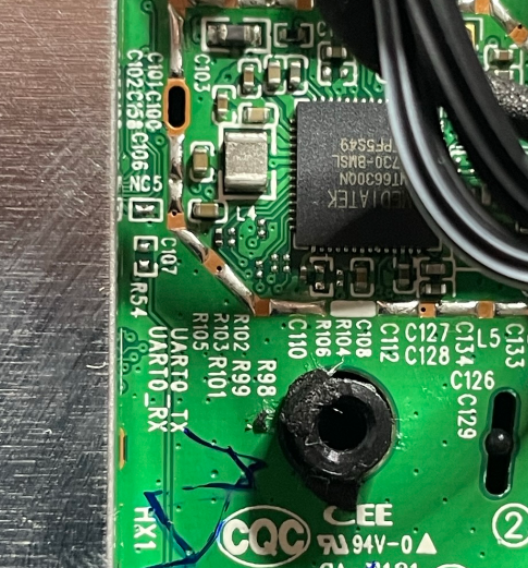
In part 3 we’ll look at where the serial port was.
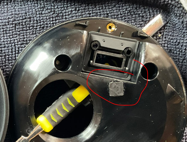
The last part of the teardown is accessing that PCB embedded in the lower part of the enclosure, supporting the micro USB power connector. On inspection there was no obvious seam, so I was trying to work out how it got there.
These things are designed for manufacture, so it shouldn’t be that hard. I also noted there was a gap where the speaker had been - in the photo, you can see that loose screw kind of nestled in it. Then it clicked, there was an inner enclosure tightly pressed in the outer. After considering whether I might try and pry it open, which is always prone to breaking tabs or other bits of plastic, in the end with some careful pressure I was able to pop it out.
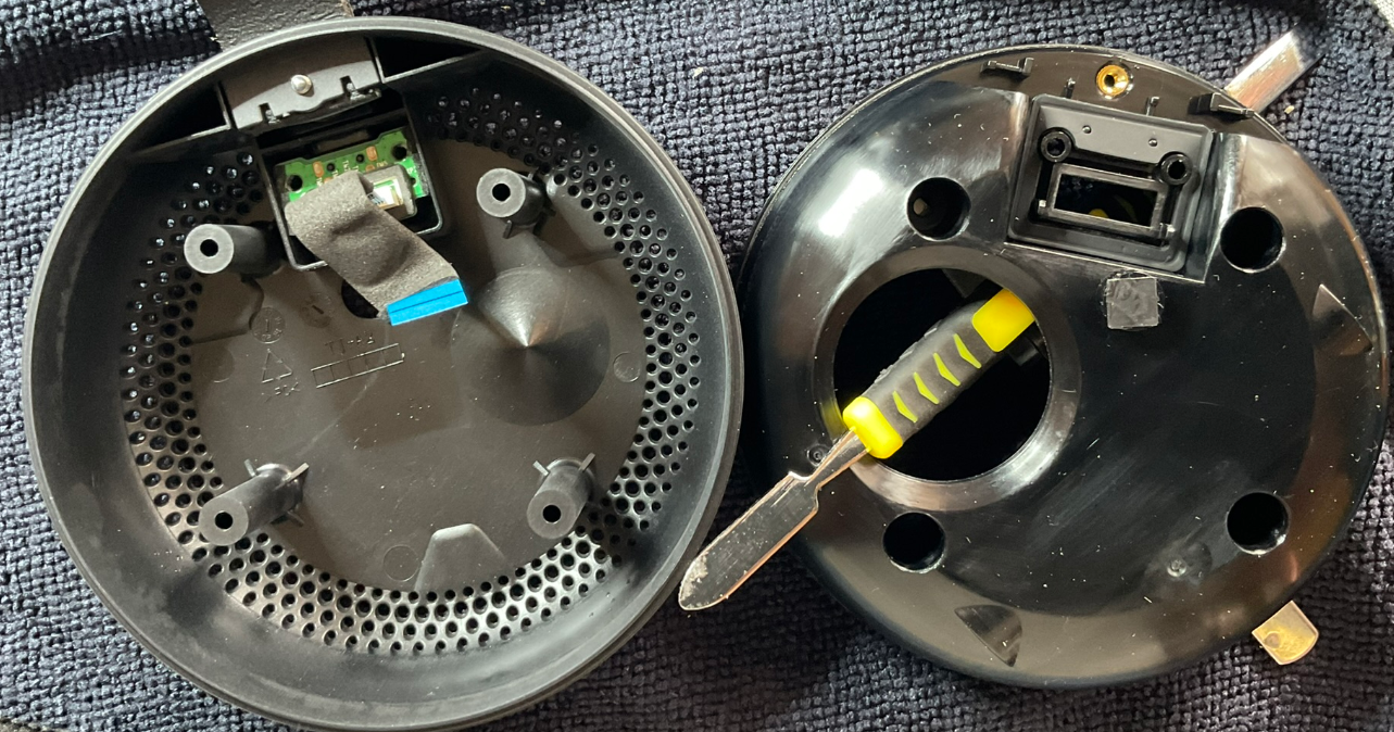
You can see the screw used to hold the strap in, it has caught on the plastic. It seems there are no smarts on the USB power PCB, just power protection.
There are also test points on the USB power PCB which could be useful in the future.
This is the end of the hardware teardown. Later we will undertake passive reconnaissance, locate the serial port and identify the makeup of the firmware.
I almost forgot, what about that sticker?
Reminder, that it would normally be further covered by the base rubber sticker…
I have a couple of hypotheses - maybe someone can enlighten me!
- as part of IPX6, perhaps the inside is temporarily evacuated when assembled to remove latent moisture?
- maybe it somehow complements the speaker? sub-woofer or damping or something?
posted in embedded, hacking, reversing, repurposing, android, hardware, home-automation
subscribe via RSS